Handle HDI Circuit Board Signal Integrity Challenges
Signal integrity is a crucial aspect of high-speed electronic systems. Signal degradation from impedance mismatches, crosstalk, ringing and ground bounce can result in transmission errors that can cause system failures. It’s therefore imperative that designers employ design procedures and simulation tools to mitigate these issues before submitting a project for fabrication. These techniques are highlighted below:
At its core, the primary goal of signal integrity is to guarantee that a transmitted interconnect signal remains an accurate depiction of the original data at its origin. This is accomplished by implementing fundamental PCB layout & routing practices that reduce signal distortion to a minimum.
To minimize signal degradation, designers must make sure that the traces used to transmit the signal remain unobstructed and close to reference planes. Assigning sufficient space for bus & escape routing is a good start, but it’s also critical to consider the specific layer configuration & clearance of the individual components. This is especially important in the case of hdi circuit board that require a complex stack-up to support high-speed interconnects. For example, placing sensitive high-speed routes on inner layers & alongside standard planes can help ensure that these signals receive the most direct & uninterrupted path possible.
How to Handle HDI Circuit Board Signal Integrity Challenges
PCB materials also play a significant role in signal integrity. Selecting the right material with a suitable dielectric constant & loss tangent can significantly impact signal propagation and attenuation. It’s also a good idea to opt for materials with excellent thermal conductivity, which will ensure effective heat dissipation and prevent thermal hotspots that can degrade signal quality.
Another crucial consideration is the management of return paths. This includes ensuring that there is enough copper in the PCB to provide a low-impedance path for return currents. Also, it’s important to place decoupling capacitors close to the IC’s pins, as this helps to minimize loop area and reduce unwanted inductance.
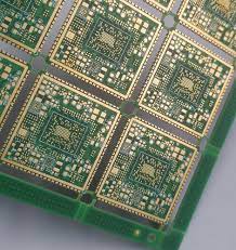
The HDI (High-Density Interconnect) circuit board stands as a pinnacle of technological advancement in the realm of electronic manufacturing. With its intricate design and compact structure, HDI circuit boards have revolutionized the way electronic devices are engineered, enabling smaller form factors, improved performance, and enhanced reliability.
At its core, the HDI circuit board embodies the principles of miniaturization and integration. Unlike traditional circuit boards, which often feature a single or double layer of conductive material sandwiched between insulating layers, HDI boards incorporate multiple layers of interconnects, vias, and microvias densely packed into a smaller footprint. This allows for the routing of signals and power across complex electronic systems with unparalleled efficiency and precision.
Finally, regular visual inspection and testing are essential to maintaining signal integrity. These inspections can help identify signal quality issues before scaling a layout for high-volume production. This can avoid costly rework & ensure that all signal traces are free from interference or distortion.