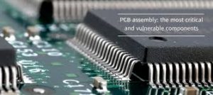
Printed Circuit Board Assembly
Printed circuit board, or PCB, assembly is the process of attaching components to the copper pads on a circuit board’s surface using either Through Hole Technology (THT) or Surface Mount Technology (SMT). This is done to create an electrical circuit that transmits signals to and from the component. These signals can be transmitted in one of two ways: via a wire or by an integrated circuit chip, which sends signals through the chip’s metal casing. Regardless of which method is used, a trained engineer must follow the schematic pattern and numbers on the silkscreen to ensure that the parts are properly installed.
The first step in the process is for a manufacturer to prepare the printed circuit board assembly by applying an adhesive layer to it. This is a crucial step because it prevents the copper from sticking to itself, which would result in faulty connections. It also helps protect the components from moisture. After the adhesive layer is applied, a stencil is placed over the board. This is a process similar to screen-printing a shirt, and it allows assemblers to apply solder paste only to certain areas of the board that will house SMTs.
Once the paste is applied, the stencil is removed and a series of holes are drilled into the laminate. Afterward, the traces that make up the circuit are etched. This removes the insulating material that separates each of the layers and exposes the copper, which is then pre-bonded to that same laminate material.
How to Printed Circuit Board Assembly
The next step in the process is for a technician to carefully inspect each of the individual layers. Depending on the complexity of the PCB, this can take anywhere from 10 to 20 minutes, but it is important for a quality product. This is because once the product emerges from the assembly line, it must have all of its resist properly covering those copper areas that are meant to remain in its final form.
Finally, the product is plated. This is the most common way to get a copper layer on a PCB. During this process, the copper is bathed in a chemical that causes it to fuse with the fiberglass substrate’s laminate. The copper is then drilled into the etched traces, and a technician examines it to make sure that no mistakes occurred during this step.
If a mistake is made, it can be difficult to find the right pin on an IC chip, so it is important to use an assembly drawing. The assembly drawing will show the placement of the pins and the numbering system that goes with them, so if a pin is lost, finding it is as simple as following the numbering on the diagram. The assembly drawing will usually have a symbol for each pin and a number, such as “R102” and “2.2K,” to help the operator locate it. This helps the assembly team avoid errors that could cause failures and delays in production.